CGS06 - Burst Generator | Cat Girl Synth
CGS06 - Burst Generator | Cat Girl Synth
Special Price
$15.30
Regular Price
$17.00
This module is a rhythm and timing accessory. It generates a burst of gate or trigger pulses at various speeds as set from a front panel control.
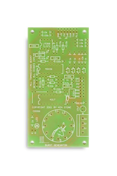
This is a PCB only suitable for multiple formats
Availability:Out of stock
BrandCat Girl Synth (CGS)


This module is a rhythm and timing accessory. It generates a burst of gate or trigger pulses at various speeds as set from a front panel control.
At higher speeds it can be used for washboard, maracas or similar rapid-burst percussive effects when connected to the appropriate sound generating device such as a ringing oscillator.
At lower speeds it can be used to step a sequencer a certain number of steps or retrigger an envelope shaper. The output pulses are quite narrow when the specified component values are used, and would best be described as trigger pulses in synths that distinguish gates from triggers. Increasing some component values will give longer gate like pulses.
How to use this module:
Experiment with it. Here's a few ideas to get you started. It can be used alone or cascaded with other burst generators. When cascaded, it could form the basis of a weird rhythm/timing generator. It could be used to step your sequencer through so many notes each down-beat. Fed to the modulation input of a VCO either directly or via an envelope shaper, it will cause a trill at the beginning of each note. It can use either its internal synchronized clock, or an external clock. It can be configured to be retriggerable or not, in which case the event in progress is concluded before it will respond to another.
A little on how it works:

The schematic of the Burst Generator.
The circuit consists of several distinct blocks. The first are the input shapers, made from IC1A and IC1B and their associated components. These take whatever signal is fed into the module and convert them to signals appropriate for driving the rest of the circuitry. With the values given, the sensitivity is set at around 1.4V, allowing triggering from signals with a +/- 10 volt swing, or with a 0V to +10 volt swing, both of which are common in modulars. The output waveforms of some modules will never fall below the 1.4V level, preventing triggering. This can be solved by increasing the value of the 10k resistor between pin 3 of IC1 and ground to 22k, or higher if needed.
IC1A is part of the circuit used to trigger the burst event. Coupled with IC1F and its associated components, it forms a "gate to trigger converter", generating a narrow positive going pulse when the "Trigger" input goes above the 1.4 volt threshold. This pulse is buffered and sent to an output jack for external use if needed. It also sends a pulse to the reset pin the 4017 via a simple AND gate. (More on this later).
IC1B is used to process the "External Clock" input. The frequency of the clock signal determines the speed of the output pulses. It can be either an external clock derived from an LFO, sequencer or similar, or from the internal clock circuit, which is normalized to the input jack.
Unlike any external clock signal, the internal clock is synchronized so that it generates a series of even length pulses when the burst generator is triggered. It has two ranges, selected by switching in or out a 330nF capacitor. The 2 meg pot specified for speed is not critical, and be anything from 1M to 5M, though obviously this will affect the range.
The output of IC1B is fed to the clock input of the 4017 decade counter, and also to an AND gate consisting of a 100k resistor and 1N4148 diode. The output of this AND gate goes to a pulse generator made from IC2E, IC2D and associated components. This pulse generator functions very similarly to the gate to trigger converter mentioned above, converting each cycle of the clock signal to a narrow pulse. This is buffered and sent to an external jack, and is the primary output of this module, namely a burst of pulses.
The 4017 decade counter forms the heart of the module. When reset, it counts up to the number selected by the switch connected to its outputs at the speed determined by the clock frequency. If we consider the rotary switch to be set to position "2" as shown in the schematic, the second clock pulse sent to the 4017 after it has been reset will present a logic HIGH to its Clock Inhibit pin (13) via the diode OR gate. This will stop the counter at that point, and any further clock pulses will be ignored. This inhibit signal is also inverted by IC2B and sent to the AND gate preventing the clock signal from reaching the second pulse generator. The inhibit signal also sends the event "End Out" output high.
The inhibit signal is reinverted and fed to another diode/resistor AND gate at the Reset input of the 4017, and another output buffer, this one for event "Duration Out". While the burst event is occurring the Clock Inhibit pin of the 4017 is held low via the 100k resistor. IC2B inverts this, presenting a HIGH to the event "Duration Out" buffer, the clock control AND gate and the input of IC2A. This will cause the output of IC2A to be LOW. If the Retrigger switch is closed, this LOW will hold the Reset pin of the 4017 LOW via the diode, preventing the event from being retriggered by any more pulses appearing on the the "Trigger" input, thus preventing retriggering of the burst.
How do the resistor/diode AND gates work? First, consider the outputs of both IC1B and IC2B to be HIGH. The input of IC2E, will be pulled HIGH via the 100k resistor. As the cathode of the diode is also being held HIGH, the diode has no effect on the input of IC2E. When the output of IC1B falls LOW, the diode will be forward biased, pulling the input of IC2E LOW with it. Alternately, if the output of IC2B is LOW when the output of IC1B is HIGH, the input of IC2E is pulled low via the 100k resistor as the diode will be reversed biased, blocking the HIGH from IC1B. When the outputs of both IC1B and IC2B are both low, it should be fairly obvious the input of IC2E will also be low. Thus, if either or both inputs are LOW, the output will also be LOW.
Summary of inputs, outputs and controls:
- External Clock - Normalized to the internal clock, but can be overridden by plugging in an external signal. Waveshape is not critical, as long as the waveform passes the trigger point.
- Trigger - Input for the external signal needed to start the event. Waveshape is not critical, as long as the waveform passes the trigger point.
- Pulses. Output for the burst event.
- Trigger Out. Output for the trigger signal derived from the Trigger input.
- Event Duration. Output. Goes high for the duration of the event. i.e. for the period the Pulses output is active
- End Out Output. Goes high when the burst event is over. This can be used to trigger another module if you wish to cascade them.
- Clock Speed. The rate at which the internal clock runs.
- Range. High and low range for the internal clock.
- Pulses. Select between 1 and 9 pulses per event.
- Retrigger. When the switch is closed, the unit cannot be retriggered during an event.
Notes:
- The length of the reset/trigger out pulse can be increased by increasing the value of the 100k resistor marked "#" on the schematic and PCB, or by increasing the value of the 10n capacitor associated with it. Increasing it too much will mess up the timing of the burst, as it will hold the reset pin of the 4017 high for the full length of this pulse.
- The length of the clock pulse presented at the "Pulses out" jack can be increased by increasing the value of the 100k resistor marked "*" on the schematic and PCB, or by increasing the value of the 10n capacitor associated with it. Increasing it too much will limit the maximum burst rate, as the pulses will all run together. If a DPDT switch is used for the "Range" function, a second capacitor could be added across the 10n capacitor when the lower speed range is selected, giving longer output pulses when most likely to be needed. The adventurous could increase the capacitor to 100n, drop the resistor to 10k, and put a 100k pot in series with it. This pot could be mounted on the panel, giving full control of the pulse length.
- The diodes and associated resistors around the internal clock oscillator disable the oscillator and prime it for the next burst when an event is over. In theory it halts the oscillator just after the beginning of its cycle. This is so when reset, a full cycle period will pass before the 4017 receives it's first clock pulse. When external clocks are used, there is no way to do this synchronizing.
- 40106/74C14 chips by different manufacturers will have different speeds. This will affect the timing of various parts of this module, though should not cause any problems, perhaps with the exception of the internal clock synchronization.
- The LED and its associated resistor are unassigned. They are there for people who cannot live without a pilot light, or something that flashes. If you don't want them, don't install them. Mine is connected with the cathode to 0V and the anode to the emitter of the transistor driving the "Duration Out" output.
- If you have separate digital and analog power supplies for your synth, connect this one to the digital supply. +/- 15 Volt Power Supply.
- The module will work on +/-12 to +/-15 volts.
- I have used BC547 transistors. These are generic NPN silicon signal transistors. Any common signal NPN should work. Emitter, Base and Collector (ebc) are marked on one transistor on the PCB to help you substitute other devices.
| Brand | Cat Girl Synth (CGS) |
|---|---|
| Additional Resources | BOM & More Information |